TI��˾��TPS51397A�ǵ�Ƭ4.5V-24V 10A��ULQ™������ͬ����ѹת����,���ɵ�MOSFET���и�Ч�ʺ�����ʹ��,���Ԫ����������,�Ӷ���ʡ�˵�Դϵͳ�Ŀռ�. TPS51397A����D-CAP3™����,�ṩ�ڲ�����������˲̬��Ӧ�ͼ��õ���·���ص���.ULQ™ (���;�̬����)�ڵ��Ĺ������ӳɵ�������м���ĺô�.�����������ѹΪ4.5V��24V,�����ѹΪ0.6V��5.5V,֧��10A�����������,0.6 V �� 1%��������(25C).���ɵ�17-m����5.9-m�� FET,ͨ��MODE���ſ�ѡ��Eco-mode™��Out-of-Audio™,500kHz��800kHz��ѡ��Ƶ��,��ѡ������ʱ��,Ĭ�ϼ��1.2ms,��ռ�ձȲ���,�����˹�������ָʾ��,��������ŵ繦��,������ڵĹ�������,�������OV��UV����,�DZ���UVLO��OT����,�������¶�-40C ��125C,23����3.0x3.0 mm HotRod™ VQFN��װ.��Ҫ���ڱʼDZ���PC����,������,�ֳ�ƽ������,��ҵPC<���������ͷֲ���Դϵͳ.���Ľ�����TPS51397A��Ҫ����,���ܿ�ͼ, 5V 10A�ο���Ƶ�·ͼ����ο������Ҫ����,�Լ�����ģ��TPS51397AEVM��Ҫ����,��·ͼ,�����嵥��PCB���ͼ.
The device is a monolithic 10-A synchronous buckconverter with integrated MOSFETs that enable highefficiency and offers ease-of-use with minimumexternal component count for space-conscious powersystems.
The TPS51397A employs D-CAP3™ control thatprovides fast transient response and excellent lineand load regulation with internal compensation. TheULQ™ (Ultra Low Quiescent) feature is extremelybeneficial for long battery life in low power operation.
The large duty operation greatly improves the loadtransient performance when input voltage is low.
The MODE pin can be used to set Eco-mode™ orOut-of-Audio™ (OOA) mode for light-load operationand 500-kHz or 800-kHz switching frequency. TheEco-mode™ maintains high efficiency during light loadoperation. The OOA mode keeps the switching
frequency above audible frequency with minimumreduction in efficiency.
The device supports both internal and external softstartoptions. It has an internal fixed soft-start time of1.2 ms.If the application needs a longer soft-starttime, the external SS pin can be connected to anexternal capacitor.
The TPS51397A integrates a power-good indicatorand provides an output discharge function. It providescomplete protection including OVP, UVP, OCP, OTP,and UVLO. The device is available in a 20-pin 3.0-mmx 3.0-mm HotRod™ package and the junction
temperature is specified from �C40C to 125C.
TPS51397A��Ҫ����:
• Input voltage range: 4.5 V to 24 V
• Output voltage range: 0.6 V to 5.5 V
• Supports 10-A continuous output current
• D-CAP3™ architecture control for fast transientresponse
• 0.6 V �� 1% feedback voltage accuracy (25C)
• Integrated 17-m�� and 5.9-m�� FETs
• ULQ™ operation (110 ��A) to enable long batterylife during system standby
• Selectable Eco-mode™ and Out-of-Audio™ byMODE pin
• 500-kHz and 800-kHz selectable switchingfrequency
• Adjustable soft-start time with default internal 1.2ms
• Large duty cycle operation
• Integrated power-good indicator
• Built-in output discharge function
• Cycle-by-cycle overcurrent protection
• Latched output OV and UV protections
• Non-latched UVLO and OT protections
• -40C to 125C Operating junction temperature
• 20-pin 3.0-mm �� 3.0-mm HotRod™ VQFN package
• Pin-to-pin compatible with 12-A TPS56C230
• Create a custom design using the TPS51397Awith the WEBENCH® Power Designer
TPS51397AӦ��:
• Notebook and PC computers
• Ultrabook, handheld tablet computers
• Industrial PC, single-board computers
• Non-military drone
• Distributed power systems
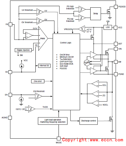
ͼ1.TPS51397A���ܿ�ͼ
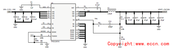
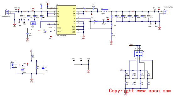
ͼ2. TPS51397A 5V 10A�ο���Ƶ�·ͼ
�ο������Ҫ����:
����ģ��TPS51397AEVM
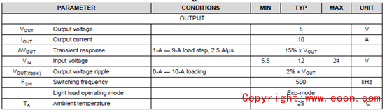
This users guide contains information for the TPS51397A evaluation module (EVM) as well as for theTPS51397A DC/DC converter. Also included are the performance specifications, schematic, layout and, the billof materials for the TPS51397AEVM.
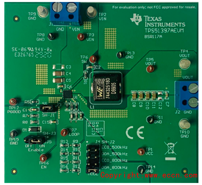
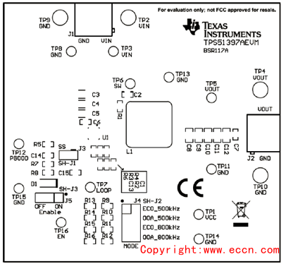
ͼ3.����ģ��TPS51397AEVM����ͼ(����)
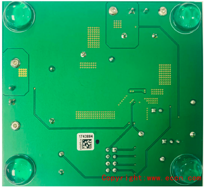
ͼ4.����ģ��TPS51397AEVM����ͼ(����)
ͼ5.����ģ��TPS51397AEVM��·ͼ
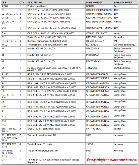
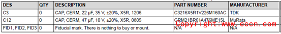
����ģ��TPS51397AEVM�����嵥:
ͼ6.����ģ��TPS51397AEVM PCB���ͼ(1):����װ��
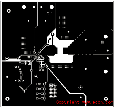
ͼ7.����ģ��TPS51397AEVM PCB���ͼ(2):����
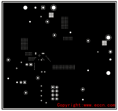
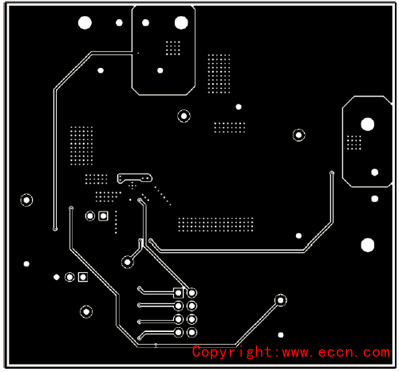
ͼ8.����ģ��TPS51397AEVM PCB���ͼ(3):��1
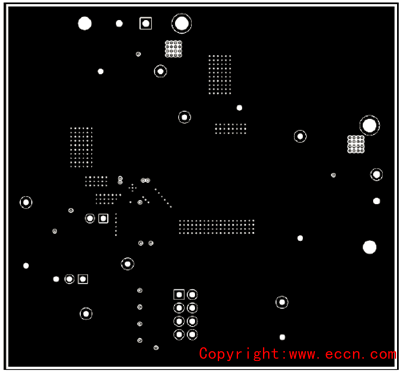
ͼ9.����ģ��TPS51397AEVM PCB���ͼ(4):��2
ͼ10.����ģ��TPS51397AEVM PCB���ͼ(5):�ײ�