 |
|
| |
|
|
ҵ��Ǣ̸��
��ϵ�ˣ���˳ƽ
�ֻ���17727550196����ͬ�ţ�
QQ:3003262363
EMAIL:zsp2018@szczkjgs.com
��ϵ�ˣ�۳�Ȼ�
�ֻ���17727552449 ����ͬ�ţ�
QQ:2850985542
EMAIL:yanxianhui@szczkjgs.com
���������緽ʽ��
�ֻ���13713728695����ͬ�ţ�
QQ:3003207580
EMAIL:panbo@szczkjgs.com
��ϵ�ˣ��˲� |
|
|
| |
|
 |
|
 |
��ǰλ�ã���ҳ -> �������� |
|
|
| DRV8876 N��H����������������� |
|
|
| ������Դ���������Ƽ� ����ʱ�䣺2019/8/24 9:34:00 |
|
TI��˾��DRV8876�������ڸ����ն�Ӧ�õ�������������������,������N��H��,��ɱ���ѹ��,�������͵���,�������������������·.��ɱ������߱ߺ͵ͱ�N��MOSFET��֧��100%ռ�հױȶ������Ч��.���ɵĵ������ʹ���������ܵ�����ʱ�ʹ���ʱ���������.������ͨ���ɵ��ⲿ����ѹ���趨.����������һ��˫����ˢDC����,������������ˢDC�����Լ���������͵�и���,������ѹ4.5V-37V,���������ֵ��3.5A,PH/EN��PWM H�ſ���ģʽ,�������ſ���ģʽ,֧��1.8V,3.3V��5V������,������˯��ģʽ:<1-��A @ VVM = 24-V, TJ = 25��.���ɵı���������Ƿѹ��ס(UVLO),��ɱ�Ƿѹ(CPUV),����������(OCP),�ȹض�(TSD),�Զ����ϻָ�����ָ������(nFAULT).��Ҫ���ڴ��ͺ�С�ͼ��õ���,��ӡ����ɨ����,�����DZ�,ATM,�ֳ��㳮����EPOS�Լ��ŷ�����ͼ�����,������,���κ��������.���Ľ�����DRV887xϵ����Ҫ����,���ܿ�ͼ,Ӧ�õ�·,�Լ�����ģ��DRV8876x/74xEV��Ҫ����,��·ͼ,�����嵥��PCB���ͼ.
The DRV887x family of devices are flexible motordrivers for a wide variety of end applications. Thedevices integrate an N-channel H-bridge, chargepump regulator, current sensing and regulation,current proportional output, and protection circuitry.
The charge pump improves efficiency by allowing forboth high-side and low-side N-channels MOSFETsand 100% duty cycle support. The family of devicescome in pin to pin, scalable RDS(on) options to supportdifferent loads with minimal design changes.
Integrated current sensing allows for the driver toregulate the motor current during start up and highload events. A current limit can be set with anadjustable external voltage reference. Additionally,the devices provide an output current proportional tothe motor load current. This can be used to detectmotor stall or change in load conditions. Theintegrated current sensing uses an internal currentmirror architecture, removing the need for a largepower shunt resistor, saving board area and reducingsystem cost.
A low-power sleep mode is provided to achieve ultralowquiescent current draw by shutting down most ofthe internal circuitry. Internal protection features areprovided for supply undervoltage lockout (UVLO),charge pump undervoltage (CPUV), outputovercurrent (OCP), and device overtemperature(TSD). Fault conditions are indicated on nFAULT.
DRV887xϵ����Ҫ����:
1• N-channel H-bridge motor driver
�C Drives one bidirectional brushed DC motor
�C Two unidirectional brushed DC motors
�C Other resistive and inductive loads
• 4.5-V to 37-V operating supply voltage range
• High output current capability
�C DRV8876: 3.5-A Peak
• Integrated current sensing and regulation
• Proportional current output (IPROPI)
• Selectable current regulation (IMODE)
�C Cycle-by-cycle or fixed off time
• Selectable input control modes (PMODE)
�C PH/EN and PWM H-bridge control modes
�C Independent half-bridge control mode
• Supports 1.8-V, 3.3-V, and 5-V logic inputs
• Ultra low-power sleep mode
�C <1-��A @ VVM = 24-V, TJ = 25��
• Spread spectrum clocking For lowelectromagnetic interference (EMI)
• Integrated protection features
�C Undervoltage lockout (UVLO)
�C Charge pump undervoltage (CPUV)
�C Overcurrent protection (OCP)
�C Thermal shutdown (TSD)
�C Automatic fault recovery
�C Fault indicator pin (nFAULT)
DRV887xϵ��Ӧ��:
• Brushed DC motors
• Major and small home appliances
• Vacuum, humanoid, and toy robotics
• Printers and scanners
• Smart meters
• ATMs, currency counters, and EPOS
• Servo motors and actuators
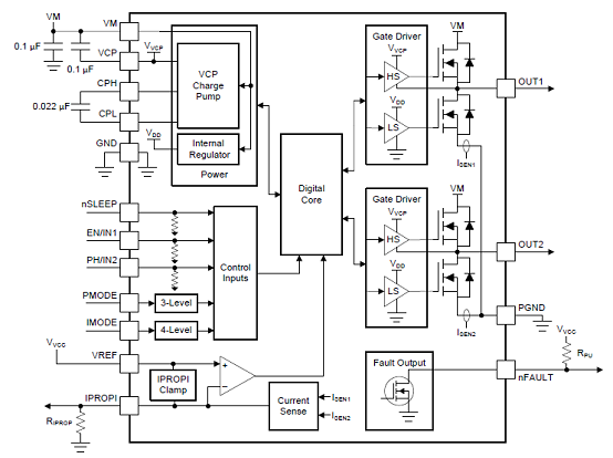
ͼ1.DRV887xϵ�й��ܿ�ͼ
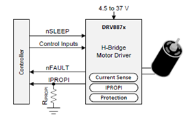
ͼ2.DRV887xϵ�м�·ͼ
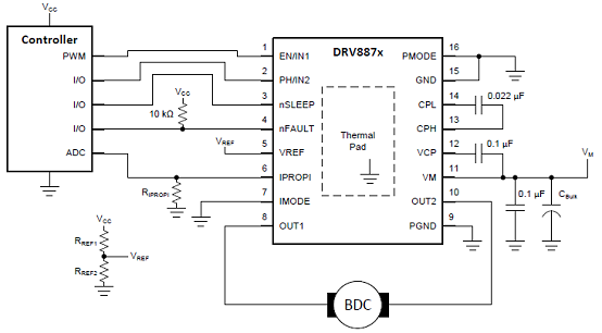
ͼ3.DRV887xϵ�е���Ӧ�õ�·ͼ(1)
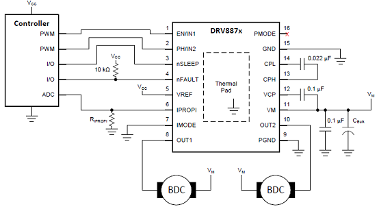
ͼ4.DRV887xϵ�е���Ӧ�õ�·ͼ(2)
����ģ��DRV8876x/74xEV
The DRV8876x/74xEVM is a complete solution for evaluating the DRV8876/74x H-bridge motor drivers. Itincludes an MSP430™ microcontroller that is preprogrammed to take input from two dedicated analogpotentiometers for PWM speed control of one or two brushed DC motors. The jumper on the PMODE pinallows the user to select from the input modes of PH/EN (GND), PWM (3.3 V), and independent halfbridgecontrol (Hi-Z). Power can be provided externally up to 37 V through the power header.
The DRV8876/74xEVM uses a single header for power entry to the EVM board. Only a single powersupply rail is necessary since an onboard 3.3-V regulator provides power to the MSP430. The minimumrecommended VM voltage for the EVM is 4.5 V and the maximum is 37 V. For complete voltage rangeinformation of the driver itself, refer to the device.
As previously mentioned, the MSP430 comes preprogrammed to control basic DC motor operation. Ifchanging the firmware via the external ez430™ development tool, do not supply power to the VMconnector on the EVM. The ez430™ board provides the necessary power during programming whenconnected to the J6 connector.
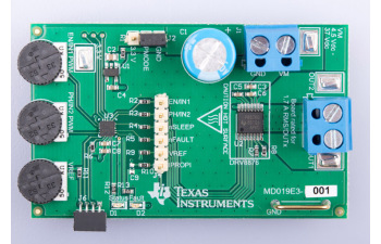
ͼ5.����ģ��DRV8876EVM����ͼ
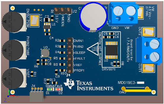
ͼ6.����ģ��DRV8876EVM PCB 3D��ͼ
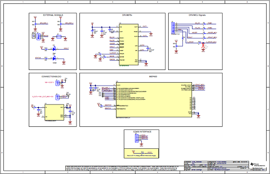
ͼ7.����ģ��DRV8876EVM��·ͼ
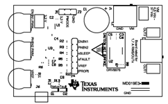
ͼ8.����ģ��DRV8876EVM PCB���ͼ(1)
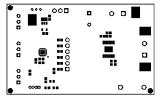
ͼ9.����ģ��DRV8876EVM PCB���ͼ(2)
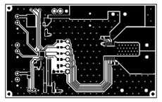
ͼ10.����ģ��DRV8876EVM PCB���ͼ(3)
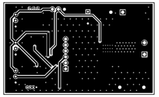
ͼ11.����ģ��DRV8876EVM PCB���ͼ(4)
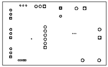
ͼ12.����ģ��DRV8876EVM PCB���ͼ(5)
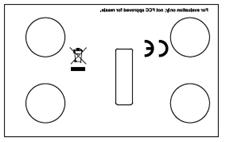
ͼ13.����ģ��DRV8876EVM PCB���ͼ(6)

ͼ14.����ģ��DRV8876EVM PCB���ͼ(7)
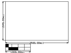
ͼ15.����ģ��DRV8876EVM PCB���ͼ(8)
|
|
| |
| |
|
|
|

