 |
|
| |
|
|
业务洽谈:
联系人:张顺平
手机:17727550196(微信同号)
QQ:3003262363
EMAIL:zsp2018@szczkjgs.com
联系人:鄢先辉
手机:17727552449 (微信同号)
QQ:2850985542
EMAIL:yanxianhui@szczkjgs.com
负责人联络方式:
手机:13713728695(微信同号)
QQ:3003207580
EMAIL:panbo@szczkjgs.com
联系人:潘波 |
|
|
| |
|
 |
|
 |
当前位置:首页 -> 方案设计 |
|
|
| ADP5301超低功耗降压调节器解决方案 |
|
|
| 文章来源: 更新时间:2015/10/13 9:05:00 |
|
ADI公司的ADP5301是超低功耗降压调节器,具有业界最高的超轻负载电源转换效率,可延长便携式设备的电池寿命,额定效率为90%,静态电流仅为180 nA,工作电压2.15V to 6.50V,非常适合物联网(IoT)应用,包括无线传感器网络和可穿戴设备如健身手环和智能手表.本文介绍了ADP5301主要特性,框图,应用电路图,以及评估板ADP5301-EVALZ主要特性,电路图,材料清单和PCB设计文件图.
The ADP5301 is high efficiency, ultralow quiescent current step-down regulator that draws only 180 nA quiescent current to regulate the output at no load. The ADP5301 runs from an input startup voltage range of 2.15 V to 6.50 V, allowing the use of multiple alkaline or NiMH, Li-Ion cells, or other power sources. The output voltage is selectable from 0.8 V to 5.0 V by an external VID resistor and factory fuse. The total solution requires only four tiny external components. The ADP5301 can operate between hysteresis mode and PWM mode via the SYNC/MODE pin.
The regulator in hysteresis mode achieves excellent efficiency at a power of less than 1 mW and provides up to 50 mA of output current. The regulator in PWM mode produces a lower output ripple and supplies up to 500 mA of output current. The flexible configuration capability during operation of the device enables very efficient power management to meet both the longest battery life and low system noise requirements. The ADP5301 contains a VOUTOK flag, which monitors the output voltage and runs at a 2 MHz switching frequency in PWM mode. SYNC/MODE can synchronize to an external clock from 1.2 MHz to 2.5 MHz. Other key features in the ADP5301 include separate enabling, QOD, and safety features such as overcurrent protection (OCP), thermal shutdown (TSD), and input undervoltage lockout (UVLO). The ADP5301 is available in 9-ball, 1.65 mm × 1.87 mm WLCSP rated for a −40℃ to +125℃ junction temperature range.
ADP5301主要特性:
Input start-up voltage range: 2.15 V to 6.50 V
Operates down to 2.00 V voltage
Ultralow 180 nA quiescent current with no load
Selectable output voltage of 1.2 V to 3.6 V or 0.8 V to 5.0 V
±1.5% output accuracy over full temperature range in PWM mode
Selectable hysteresis mode or PWM operation mode
Output current Up to 50 mA in hysteresis mode
Up to 500 mA in PWM mode
VOUTOK flag monitors the output voltage
100% duty cycle operation mode
2 MHz switching frequency with optional synchronization input from 1.2 MHz to 2.5 MHz
Quick output discharge (QOD) option
UVLO, OCP, and TSD protection
9-ball, 1.65 mm × 1.87 mm
WLCSP −40℃ to +125℃ junction temperature
ADP5301应用:
Energy (gas and water) metering
Portable and battery-powered equipment
Medical applications
Keep-alive power supplies
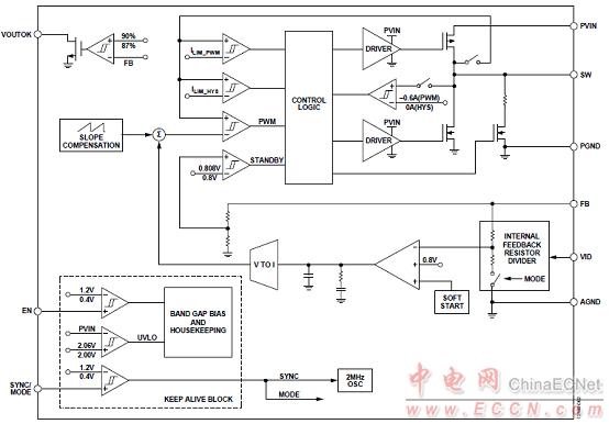
图1.ADP5301框图
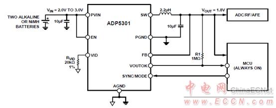
图2.采用两节碱性电池/NiMH电池ADP5301应用电路图
评估板ADP5301-EVALZ
The ADP5301 is an ultralow power, synchronous, step-down dc-to-dc regulator with a load switch in a 9-ball WLFCSP package. The ADP5301 runs from input voltages of 2.15 V to 6.50 V and requires minimal external components to provide a high efficiency solution with integrated power switch, synchronous rectifier, and internal compensation. The ADP5301-EVALZ evaluation board provides an easy way to evaluate the device. This user guide describes how to quickly set up the board to collect performance data. Complete information about the ADP5301 is available in the ADP5301 data sheet, which should be consulted in conjunction with this user guide when using the evaluation board.
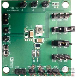
图3.评估板ADP5301-EVALZ外形图
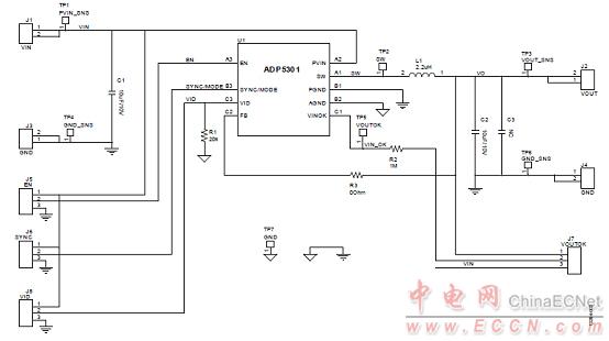
图4.评估板ADP5301-EVALZ电路图
评估板ADP5301-EVALZ材料清单:
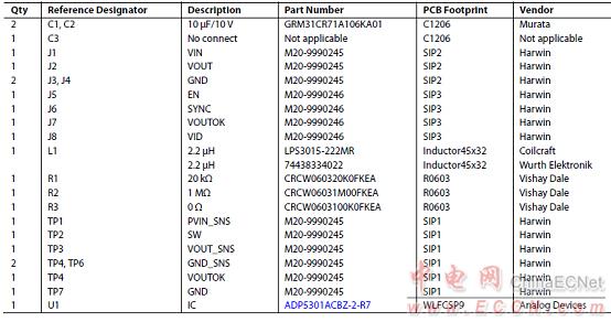

图5.评估板ADP5301-EVALZ PCB设计图(1)

图6.评估板ADP5301-EVALZ PCB设计图(2)
|
|
| |
| |
|
|
|

