 |
|
| |
|
|
ҵ��Ǣ̸��
��ϵ�ˣ���˳ƽ
�ֻ���17727550196����ͬ�ţ�
QQ:3003262363
EMAIL:zsp2018@szczkjgs.com
��ϵ�ˣ�۳�Ȼ�
�ֻ���17727552449 ����ͬ�ţ�
QQ:2850985542
EMAIL:yanxianhui@szczkjgs.com
���������緽ʽ��
�ֻ���13713728695����ͬ�ţ�
QQ:3003207580
EMAIL:panbo@szczkjgs.com
��ϵ�ˣ��˲� |
|
|
| |
|
 |
|
 |
��ǰλ�ã���ҳ -> ������� |
|
|
| MCF51AG128����BLDC���������Ʒ��� |
|
|
| ������Դ�� ����ʱ�䣺2015/9/19 9:50:00 |
|
Freescale��˾��MCF51AG128��32λColdFire������,�ں��ṩ50 MHz���ں��ٶȺ�25 MHz�������ٶ�,�ṩ����ֱ�Ӵ洢������(DMA)��iEventģ��,�ṩ����ֱ�Ӵ洢������(DMA)��iEventģ���䱸�����Ƚ������������Ƶ����������������Ϻ�ϵͳ��ȫ�������Թ���.��Ҫ�������ܼҵ��ҵӦ��.���Ľ�����MCF51AG128��Ҫ���ԺͿ�ͼ,�Լ�����MCF51AG128����������BLDC������ʾ������,��ͼ,��������ͼ�͵�·ͼ.
The MCF51AG128 is a member of the ColdFire® family of32-bit variable-length reduced instruction set (RISC)microcontroller. This document provides an overview of theMCF51AG128 series MCUs, focusing on its highlyintegrated and diverse feature set.
The MCF51AG128 derivative are low-cost, low-power, andhigh-performance 32-bit ColdFire V1 microcontroller units(MCUs) designed for industrial and appliance applications. Itis an ideal upgrade for designs based on the MC9S08AC128series of 8-bit microcontrollers.
MCF51AG128��Ҫ����:
• 32-bit Version 1 ColdFire® central processor unit (CPU)
�C Up to 50.33 MHz ColdFire CPU from 2.7 V to 5.5 V
�C Provide 0.94 Dhrystone 2.1 DMIPS per MHzperformance when running from internal RAM (0.76
DMIPS per MHz when running from flash)
�C Implements Coldfire Instruction Set Revision C(ISA_C)
• On-chip memory
�C Up to 128 KB flash memory read/program/erase overfull operating voltage and temperature
�C Up to 16 KB random access memory (RAM)
�C Security circuitry to prevent unauthorized access toRAM and flash contents
• Power-Saving Modes
�C Three ultra-low power stop modes and reduced powerwait mode
�C Peripheral clock enable register can disable clocks tounused modules, thereby reducing currents
• System Protection
�C Advanced independent clocked watchdog (WDOG)with features like, robust refresh mechanism, windowedmode, high granulation timeout, fast test of timeout, andalways forces a reset
�C Additional external watchdog monitor (EWM) to helpreset external circuits
�C Low-voltage detection with reset or interrupt
�C Separate low voltage warning with selectable trip points
�C Illegal opcode and illegal address detection with reset
�C Flash block protection for each array to preventaccidental write/erasure
�C Hardware CRC module to support fast cyclicredundancy checks
• Debug Support
�C Single-wire back ground debug interface
�C Real-time debug support, with six hardware breakpoints(4 PC, 1 address pair and 1 data) that can be configuredinto a 1- or 2-level trigger
�C On-chip trace buffer provides programmable start/stoprecording conditions
�C Support for real-time program (and optional partial data)trace using the debug visibility bus
• DMA Controller
�C Four independently programmable DMA channelsprovide the means to directly transfer data betweensystem memory and I/O peripherals
�C DMA enabled peripherals include IIC, SCI, SPI, FTM,HSCMP, ADC, RTC, and eGPIO, and the DMA requestfrom these peripherals can be configured as DMAsource or as an iEvent input
• CF1_INTC
�C Support of 44 peripheral I/O interrupt requests and sevensoftware (one per level) interrupt requests
�C Fixed association between interrupt request source, leveland priority, up to two requests can be remapped to thehighest maskable level and priority
�C Unique vector number for each interrupt source
�C Support for service routine interrupt acknowledge(software IACK) read cycles for improved system
performance
�C Ability to mask any individual or all interrupt sources
• System Clock Sources
�C Oscillator (XOSC) �� Loop-control pierce oscillator; crystal or ceramic resonator range of 31.25 kHz to 38.4 kHz or 1MHz to 16 MHz
�C Internal Clock Source (ICS) �� Frequency-locked-loop (FLL) controlled by internal or external eference; trimmableinternal reference allows 0.2% resolution and 2% deviation (1% across 0 to 70 ºC)
• Peripherals
�C ADC �� 24 analog inputs with 12 bits resolution; output formatted in 12-, 10- or 8-bit right-justified format; single orcontinuous conversion (automatic return to idle after single conversion); interrupt or DMA request when conversioncomplete; operation in low-power modes for lower noise operation; asynchronous clock source for lower noise operation;selectable asynchronous hardware conversion triggers from RTC, PDB, or iEvent; dual samples based on hardwaretriggers during ping-pong mode; on-chip temperature sensor
�C PDB �� 16-bit of resolution with prescaler; seven possible trigger events input; positive transition of trigger event signalinitiates the counter; support continuous trigger or single shot, bypass mode; supports two triggered delay outputs or ORedtogether; pulsed output could be used for HSCMP windowing signal
�C iEvent �� User programmable combinational boolean output using the four selected iEvent input channels for use asinterrupt requests, DMA transfer requests, or hardware triggers
�C FTM �� Two 6-channel flexible timer/PWM modules with DMA request option; deadtime insertion is available for eachcomplementary channel pair; channels operate as pairs with equal outputs, pairs with complimentary outputs orindependent channels (with independent outputs); 16-bit free-running counter; the load of the FTM registers which havewrite buffer can be synchronized; write protection for critical registers; backwards compatible with TPM
�C TPM �� 16-bit free-running or modulo up/down count operation; two channels, each channel may be input capture, outputcompare, or edge-aligned PWM; one interrupt per channel plus terminal count interrupt
�C CRC �� High speed hardware CRC generator circuit using 16-bit shift register; CRC16-CCITT compliancy with x16 + x12+ x5 + 1 polynomial; error detection for all single, double, odd, and most multi-bit errors; programmable initial seed value
�C HSCMP �� Two analog comparators with selectable interrupt on rising edge, falling edge, or either edges of comparatoroutput; the positive and negative inputs of the comparator are both driven from 4-to-1 muxes; programmable voltagereference from two internal DACs; support DMA transfer
�C IIC �� Compatible with IIC bus standard and SMBus version 2 features; up to 100 kbps with maximum bus loading;multi-master operation; software programmable for one of 64 different serial clock frequencies; programmable slaveaddress and glitch input filter; interrupt driven byte-by-byte data transfer; arbitration lost interrupt with automatic modeswitching from master to slave; calling address identification interrupt; bus busy detection; broadcast and 10-bit addressextension; address matching causes wake-up when MCU is in Stop3 mode; DMA support
�C SCI �� Two serial communications interface modules with optional 13-bit break; full-duplex, standard non-return-to-zero(NRZ) format; double-buffered transmitter and receiver with separate enables; 13-bit baud rate selection with /32fractional divide; interrupt-driven or polled operation; hardware parity generation and checking; programmable 8-bit or9-bit character length; receiver wakeup by idle-line or address-mark; address match feature in receiver to reduceaddress-mark wakeup ISR overhead; 1/16 bit-time noise detection; DMA transmission for both transmit and receive
�C SPI �� Two serial peripheral interfaces with full-duplex or single-wire bidirectional option; double-buffered transmitterand receiver; master or slave mode operation; selectable MSB-first or LSB-first shifting; 8-bit or 16-bit data modes;programmable transmit bit rate; receive data buffer hardware match feature; DMA transmission for transmit and receive
• Input/Output
�C Up to 69 GPIOs and one Input-only pin
�C Interrupt or DMA request with selectable polarity on all input pins
�C Programmable glitch filter, hysteresis and configurable pull up/down device on all input pins
�C Configurable slew rate and drive strength on all output pins
�C Independent pin value register to read logic level on digital pin
�C Up to 16 rapid general purpose I/O (RGPIO) pins connected to the processor��s local 32-bit platform bus with set, clear,and faster toggle functionality
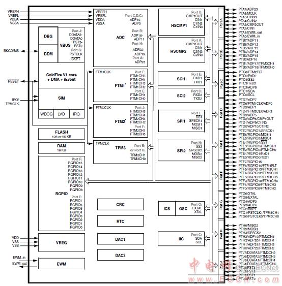
ͼ1. MCF51AG128ϵ��MCU��ͼ
����MCF51AG128����������BLDC������ʾ��
3-Phase BLDC Sensorless Control using MCF51AG128
This design reference manual describes the design of a sensorless 3-phase Brushless DC (BLDC) motordrive based on Freescale��s 32-bit MCF51AG128 control device.
BLDC motors are very popular in a wide application area. The BLDC motor lacks a commutator and istherefore more reliable than the DC motor. The BLDC motor also has advantages when compared to anAC induction motor. Because it achieves a higher efficiency by generating the rotor magnetic flux withrotor magnets, a BLDC motor is used in high-end white goods (such as refrigerators, washing machines,dishwashers), high-end pumps, fans and in other appliances which require a high reliability and efficiency.
The concept of the application is a speed and torque closed-loop BLDC drive using a sensorless BEMFzero crossing technique. It serves as an example of a BLDC motor control design using a FreescaleColdFire V1 Family MCU.
This reference design includes basic motor theory, system design concept, hardware implementation, andsoftware design, including the FreeMASTER software visualization tool.
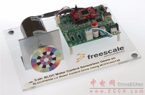
ͼ2.����MCF51AG128����������BLDC������ʾ������ͼ
The motor control system is designed to drive a 3-phase Brushless DC Motor (BLDC Motor) in acombined speed/torque closed-loop. The application meets the following performance specifications:
• Sensorless Brushless DC Motor Control by Back-EMF zero-crossing sensing
• Targeted at the MCF51AGx platform
• Running on a low voltage (24 V) 3-phase Motor Control Drive board
• Control technique incorporates:
�� Sensorless control with the combined speed/torque closed-loop
�� Using an ADC for zero-crossing sensing
�� Rotation in both directions
�� Full 4-quadrant operation
�� Start from any motor position with rotor alignment
�� Manual interface (Direction switch, Up/Down push button control)
�� FreeMASTER software control interface (motor run/stop, speed/torque set-up)
�� FreeMASTER software remote monitor
�� MCU initialization is done by Device Initialization tool (part of Processor Expert)
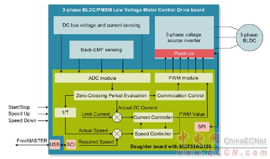
ͼ3.����BLDC/PMSM��ѹ�����������ͼ
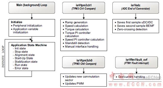
ͼ4.����������ͼ
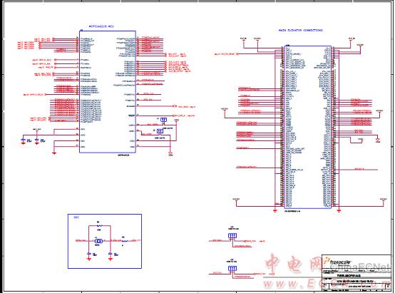
ͼ5.����MCF51AG128����������BLDC������ʾ���·ͼ(1)
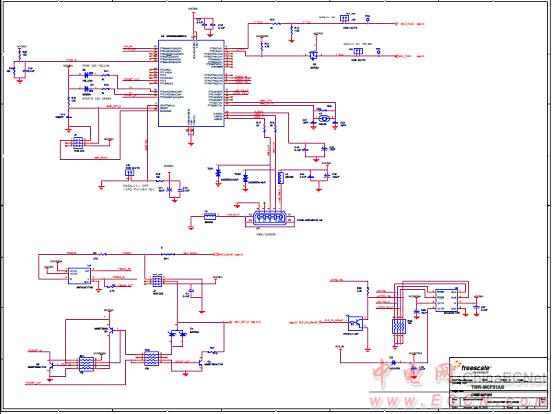
ͼ6.����MCF51AG128����������BLDC������ʾ���·ͼ(2)
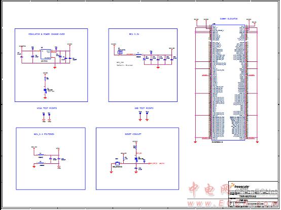
ͼ7.����MCF51AG128����������BLDC������ʾ���·ͼ(3)
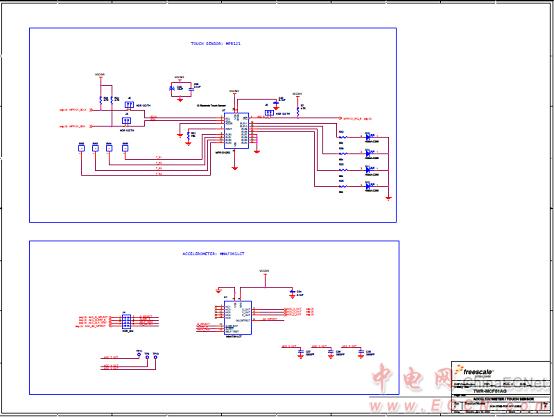
ͼ8.����MCF51AG128����������BLDC������ʾ���·ͼ(4)
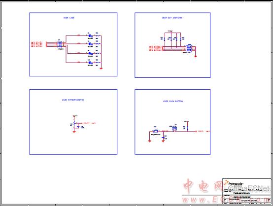
ͼ9.����MCF51AG128����������BLDC������ʾ���·ͼ(5)
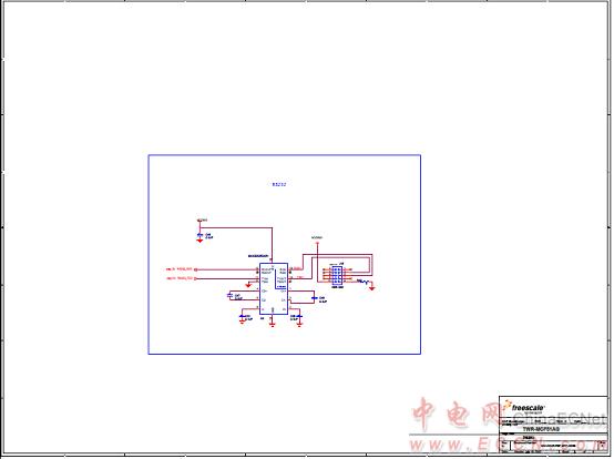
ͼ10.����MCF51AG128����������BLDC������ʾ���·ͼ(6) |
|
| |
| |
|
|
|

